





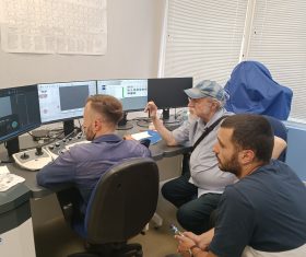
Microscopy and Microanalysis

Project Description: 

CANDLE Synchrotron Research Institute provides a range of microscopy and microstructural characterization capabilities for the investigation of biological, inorganic, and engineering materials. The available infrastructure combines advanced optical microscopy, metallographic microscopy, and scanning electron microscopy, allowing samples to be investigated at different spatial scales and using complementary characterization approaches. Optical microscopy capabilities include two-photon fluorescence laser scanning microscopy, which enables high-resolution three-dimensional imaging of fluorescently labeled specimens and investigation of structures at different depths. Metallographic microscopy is used for detailed examination of prepared material cross-sections, microstructures, phases, defects, and interfaces. Scanning electron microscopy with the ZEISS EVO 10 provides high-resolution surface imaging and elemental analysis of a broad range of organic and inorganic samples, with magnification from 7× to 1,000,000×. These complementary techniques enable comprehensive characterization of morphology, microstructure, surface features, and composition and support research in materials science, nanotechnology, biology, biomedicine, physics, electronics, optics, and engineering.

Applications
  1. Optical Microscopy – Two-Photon Fluorescence Laser Scanning Microscopy
  • Fluorescence imaging of biological samples
  • Three-dimensional imaging of biological structures
  • Live-cell and tissue studies
  • Cellular and subcellular structure investigation
  • Imaging of fluorescently labeled specimens
  • Investigation of biological processes and dynamics
  • Medical and biomedical research
  • Biochemistry, genetics, histology, and microbiology
  • Investigation of samples at different depths
  1. Metallographic Microscopy – MMT-1600B
  • Metallographic examination of metallic materials
  • Microstructure characterization
  • Grain and phase structure investigation
  • Analysis of material interfaces
  • Investigation of defects and inclusions
  • Examination of welded and brazed joints
  • Cross-sectional analysis of metallic samples
  • Investigation of deformation and structural changes
  • Quality control and materials research
  1. Scanning Electron Microscopy – ZEISS EVO 10
  • High-resolution surface morphology analysis
  • Micro- and nanoscale structure characterization
  • Surface defect investigation
  • Elemental composition analysis
  • Investigation of organic and inorganic materials
  • Particle and surface-feature characterization
  • Materials science and nanotechnology research
  • Biological and biomedical research
  • Electronics and optics research
  • Engineering and surface analysis
Specifications

Optical Microscopy

  • Two-photon fluorescence laser scanning microscopy
  • Excitation wavelength: 1030 nm
  • Pulse energy: up to 25 nJ
  • Pulse duration: approximately 280 fs
  • Three-dimensional x-y-z scanning
  • Fluorescence-based imaging
  • Optical sectioning of specimens
  • Infrared laser excitation

Metallographic Microscopy

  • Instrument: MMT-1600B
  • Optical metallographic microscopy
  • Suitable for prepared metallographic sections
  • High-magnification microstructure observation
  • Suitable for metallic materials and engineering samples
  • Digital imaging capability can be integrated with a microscope camera system

Scanning Electron Microscopy

  • Instrument: ZEISS EVO 10
  • Scanning electron microscopy
  • Magnification: 7×–1,000,000×
  • High-resolution surface imaging
  • Secondary and backscattered electron imaging capabilities
  • Elemental analysis capability
  • Suitable for organic and inorganic samples
  • Reduced sample-preparation requirements
  • Digital image acquisition
Advantages

Optical Microscopy

  • Non-invasive and minimally destructive imaging
  • Three-dimensional visualization of specimens
  • High sensitivity for fluorescently labeled structures
  • Ability to investigate structures beneath the sample surface
  • Reduced phototoxicity compared with conventional single-photon excitation in appropriate applications

Metallographic Microscopy

  • Direct investigation of prepared material cross-sections
  • Effective characterization of metallic microstructures
  • Suitable for phase, grain, defect, and interface analysis
  • Complementary to mechanical and materials testing
  • Useful for comparative examination before and after processing or testing

Scanning Electron Microscopy

  • Very wide magnification range
  • High-resolution surface characterization
  • Morphology and composition can be investigated
  • Suitable for a broad range of organic and inorganic samples
  • Different detectors provide complementary information
  • Relatively simple and rapid sample preparation for many applications
Limitations

Optical Microscopy

  • Fluorescence imaging requires suitable fluorescent labels or naturally fluorescent samples
  • Optical penetration depth depends on the sample properties
  • Multiphoton imaging requires appropriate laser excitation and optical conditions
  • High-quality three-dimensional imaging may require careful sample preparation

Metallographic Microscopy

  • Samples generally require cutting, mounting, grinding, polishing, and, where appropriate, etching
  • The technique is primarily suitable for surface or cross-sectional examination
  • Results depend strongly on sample preparation quality
  • Internal structures cannot be directly investigated without preparing an appropriate cross-section

Scanning Electron Microscopy

  • Sample dimensions are limited by the SEM chamber and specimen stage
  • Conventional high-vacuum operation may require vacuum-compatible samples
  • Non-conductive samples may require appropriate preparation or low-vacuum operation
  • Electron-beam-sensitive materials may be affected during prolonged observation
  • Elemental analysis depends on the installed detector configuration and sample characteristics
Status
  • Research / Operation
  • Available for CANDLE SRI research activities and external users upon coordination
Patents

Contact Person:

Dr. Arsham Yeremyan, PhD

Position:

Head of Photon Beams and Optics group

Phone: +37498817264