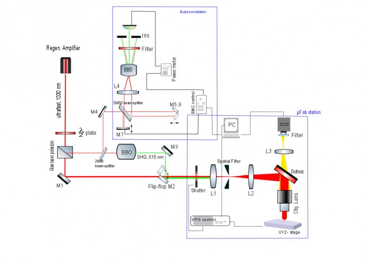


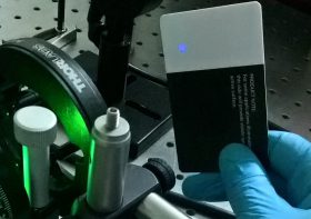
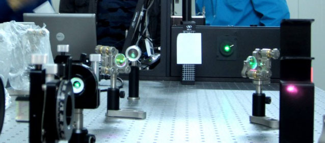
The microfabrication station of DELTA is a femtosecond laser-based micro-machining system dedicated to ultrafast materials processing and fabrication of micro- and nano-devices for a vast variety of scientific and R&D applications.
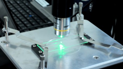
The system is an integration of the Newport’s µFAB™ station and the Amplitude Systemes high-energy, ultrashort “s-pulse” laser. Combined with sample motion/positioning and pulse-parameter control units and software, the station represents an entire lab on an optical table.
Features
- Ultrafast processing reduces the heat affected zones and improves the quality and resolution for nanoscale fabrication
- High accuracy of XYZ positioning/motion and high-grade optics to achieve nanoscale precision in both 2D and 3D processing
- Unique flexibility of laser parameters allow the processing of virtually any material by utilizing the relevant process and approach (laser-induced modification of chemical and optical properties, selective material removal, etc.)
- Extremely high laser intensities can be used for multiphoton absorption and processing of otherwise transparent materials with even smaller feature sizes
- Software for both visualization of the machining process and direct control of sample motion hardware and pulse parameters.
Specifications
- Pulse duration: from 400 fs to 10 ps
- Repetition rate: from 1 Hz to 100 kHz
- Average power: up to 8 W
- Pulse energy: up to 2 mJ (1030 nm) and 1 mJ (515 nm)
- Wavelengths 1030 nm, 515 nm
- Sample positioning accuracy: ±50 nm
- Travel range: 100 x 100 mm (XY), 25 mm (Z)
Applications
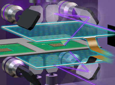
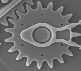
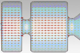
- Direct laser writing (DLW) of 2D patterns of micro- and nanostructures
- 3D microfabrication: photonics, microelectronics, micro-electromechanical systems (MEMS)
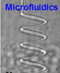
- Optical interconnects, diffraction gratings, microfluidics, sensors, labs-on-a-chip
- refractive index modification inside the bulk of material; 3D (volume) writing of waveguides in semiconductors and dielectrics;
- Laser ablation, material transferring, drilling, marking, dicing, cutting, trimming, milling, scribing, selective etching, laser-induced modification of chemical and optical properties
- Processing of practically all materials: metals, semiconductors, glasses, polymers, ceramics, and biological samples
- Fabrication of prototype devices and elements with specific functionality
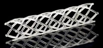
- Bio-medical: fine texturing of bio-samples, bioresorbable coronary stents, etc.

Ultrafast laser processing of materials has become a fast growing field of research and technology due to the unique capabilities coming from fundamentally new mechanisms of laser-matter interaction.
At least two aspects of femtosecond laser processing make it advantageous compared with conventional, longer-pulse laser techniques. Suppression of heat diffusion to surrounding regions during the ultrafast processing improves the quality and spatial resolution for nanoscale processing. Furthermore, the high peak intensities of ultrashort pulses increase the probability of multiphoton absorption in otherwise transparent materials, so that both surface (2D) and volume (3D) writing of micro- and nanostructures becomes feasible.
The microfabrication station is operated by “s-pulse” femtosecond laser which has a unique flexibility of pulse parameters like energy, repetition rate and pulse duration. Depending on the specific application, IR (1030 nm) or green (SHG, 515 nm) can be selected for optimized processing.
Combined with high-precision, PC-controlled µFAB station the system allows direct laser writing (DLW) of 2D patterns of micro- and nanostructures, as well as 3D (volume) structures with specific functionality for a variety of applications such as diffraction gratings, sensors, optical interconnects and waveguides, microfluidic devices to mention just a few.