


March 12, 2015
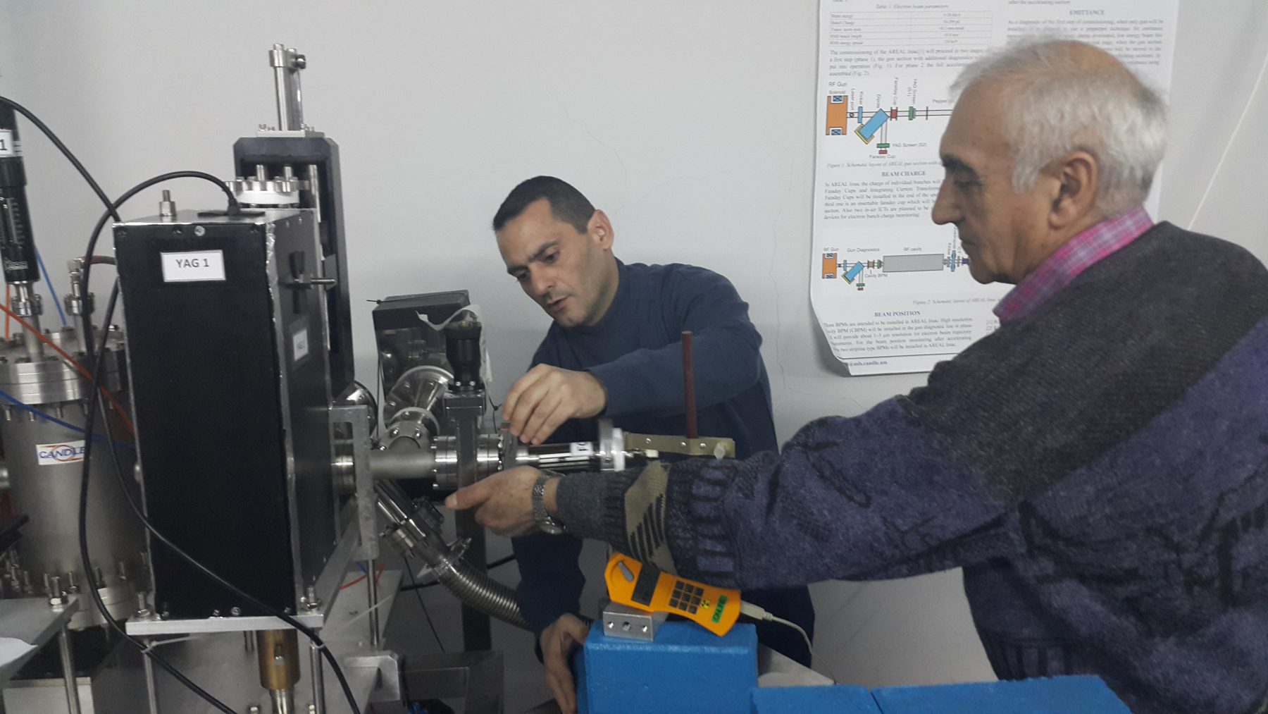
The research group from Alikhanyan National Science Laboratory (Yerevan Physics Institute) headed by Prof. H. Yeritsyan reported about the new experimental results on the AREAL accelerator within the framework of the project “Study of Electro-physical Properties of Silicon and Silicon-dielectric Structures”.
The radiation defect formation of the Silicon single crystals was observed after irradiation of the samples by 3,5 MeV energy AREAL electron beam. The last known experimental data predict that the cluster radiation defects formation in Si crystals takes place at irradiation of the sample with electron beams with energy higher than 10 MeV, whereas at lower energies mainly point pair defects are created. The radiation defect formation in Si crystal at 3,5 MeV energy is unusual for these electron energies and most likely is the cluster type defects caused by the AREAL subpicosecond electron pulses (charge per pulse 200 pC). This preliminary conclusion was reached after measurements of main electro-physical parameters of n-Si crystals: electro-conductivity, Hall mobility and main charge carriers concentration. After the Si samples irradiation, the Hall mobility has decreased almost twice, which suggests the presence of strong scattering mechanism for carrier’s mobility such as cluster type defects.